The PCF8591 is a monolithically integrated, and a separate power supply, low-power, 8-bit CMOS data acquisition devices. The PCF8591 has the four analog inputs, one analog output and a serial I2C bus interface.
PCF8591 three address pins A0, A1 and A2 can be used in hardware address programmed 8 PCF8591 device allows access to the same I2C bus, without the need for additional hardware. On the PCF8591 device input and output of the address, control and data signals are transmitted in serial fashion via the two-wire bidirectional I2C bus.
PCF8591 Features
- Single power supply
- PCF8591 operating voltage range of 2.5V-6V
- Via I2C bus serial input / output
- PCF8591 by 3 hardware address pins addressing
- PCF8591 I2C bus speed sampling rate decided
- 4 analog inputs programmable single-ended or differential input
- Automatic incremental channel selection
- PCF8591 analog voltage range from VSS to VDD
- PCF8591 built-in track-and-hold circuit
- 8-bit successive approximation A / D converter
- 1 analog output DAC gain
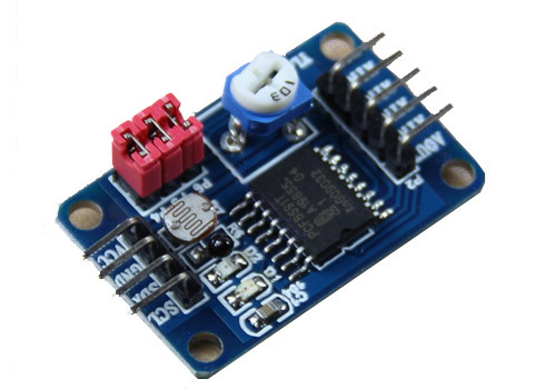
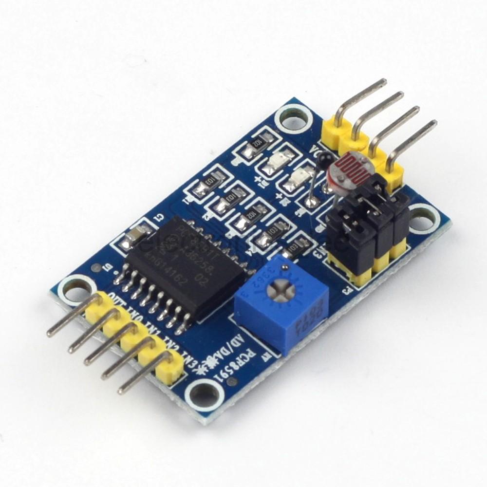
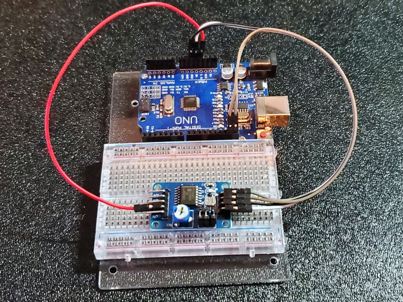
The easiest way as usual is to purchase a module, I found this interesting one which had integrated devices which can be used to test the analog inputs
Features
- Module supports external voltage input of the 4-way acquisition (voltage input range of 0-5v)
- integrated photoresistor
- integrated thermistor
- integrated potentiometer
- Modules power indicator
- Modules with DA output indicator, when the module DA output interface voltage reaches a certain value, will be lit panel the DA output indicator, the higher the voltage, the more obvious indicator brightness
- Remove shunts to bypass on board integrated devices
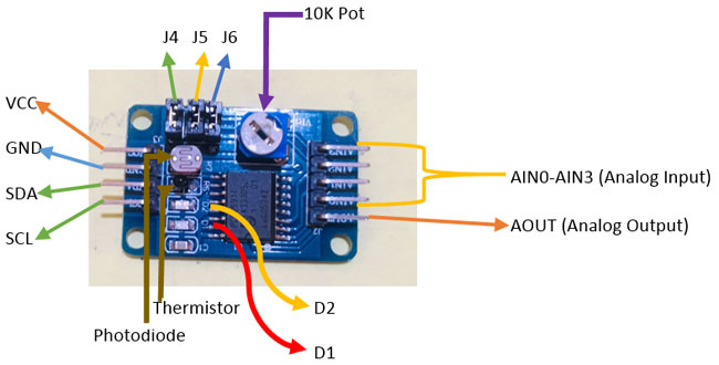
The left connector
- AOUT chip DA output interface
- AINO chip analog input interface 0
- AIN1 chip analog input interface 1
- AIN2 chip analog input interface 2
- AIN3 chip analog input interface 3
The right connector
- SCL
- SDA
- GND
- VCC – connected to 3.3v-5v
PCF8591 module functions
| Control | Register | Function | On board Device |
|---|---|---|---|
| 0 | channel 0 | Read ADC 0 | LDR |
| 1 | channel 1 | Read ADC 1 | NTC THERMISTOR |
| 2 | channel 2 | Read ADC 2 | NC |
| 3 | channel 3 | Read ADC 3 | POTENTIOMETER |
| +64 | analog OE | DAC output | O/P LED |
The O/P LED will begin to turn on with the output set to 140 or more with VCC at 3v3.
Code
#include "Wire.h"
#define PCF8591 (0x90 >> 1)
byte adcvalue0, adcvalue1, adcvalue2, adcvalue3;

void setup()
{
 Wire.begin();
 Serial.begin(9600);
}

void loop()
{
 Wire.beginTransmission(PCF8591);
 Wire.write(0x04);
 Wire.endTransmission();
 Wire.requestFrom(PCF8591, 5);

 adcvalue0=Wire.read();
 adcvalue0=Wire.read();
 adcvalue1=Wire.read();
 adcvalue2=Wire.read();
 adcvalue3=Wire.read();

 Serial.print(adcvalue0);
 Serial.print(" ,");
 Serial.print(adcvalue1);
 Serial.print(" ,");
 Serial.print(adcvalue2);
 Serial.print(" ,");
 Serial.print(adcvalue3);
 Serial.println();

 delay(1000);
}
DAC Analog Output
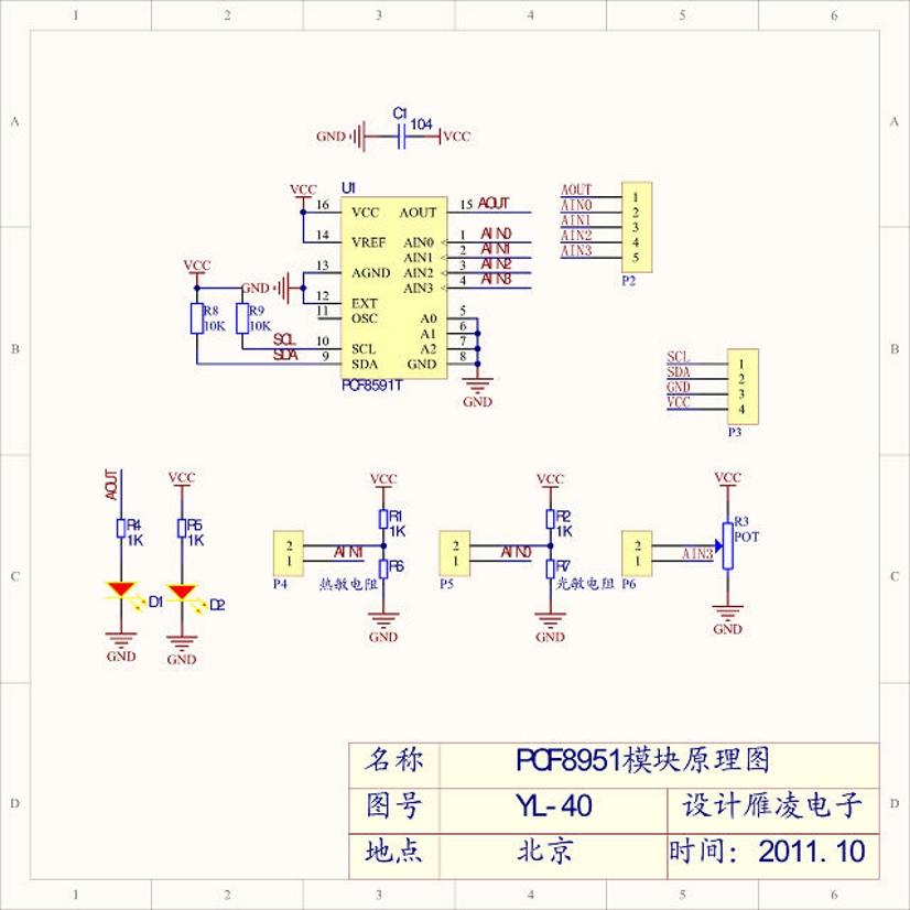
The DAC output is connected to pin AOUT.
The 8-bit single output provides 256 steps of resolution. For a VCC of 5V, the step size will be 5V/256 = 20mV.
The DAC output has a modest current capability to begin with and also has a 1K resistor and LED hooked up to it. The LED makes it easy to see the affect of changing the analog output for experimenting, but for use in actual applications it limits the output swing from reaching full Vcc. If Vcc is 5V, it will max out at about 4.2V. For applications that need the full GND to Vcc swing of the DAC output it is recommended to remove the LED to avoid the extra load on the output.
The DAC is also used internally by the ADC inputs. If using the DAC output, a track-and-hold circuit keeps the value that was set on the output pin while the DAC circuit is being used by the ADC circuit.
ADC Analog Inputs
The 4 analog inputs connect to the header pins AIN0-AIN3 and can be used as 4 general purpose analog inputs. By default these are 4 single-ended inputs referenced to ground. The PCF8591 chip also supports using them as 2 differential inputs. Refer to the datasheet for specifics on using that mode.
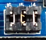
There are 3 jumpers installed on the module that alternatively connects an on-board LDR, thermistor and potentiometer to 3 of these 4 inputs as follows. If you want to use those inputs as general purpose inputs, the jumper should be removed from that location.
J5 – Connects LDR to channel 0 (AIN0)
J4 – Connects thermistor to channel 1 (AIN1)
J6 – Connects the potentiometer to channel 3 (AIN3)
Note that channel 2 (AIN2) does not have an alternate purpose, so no jumper is necessary.
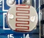
LDR – The Light Detecting Resistor (LDR) can detect basic changes in the intensity of the light striking it.
A decrease in the amount of light hitting the sensor will cause an increase in the voltage on channel 0.
The LDR is useful for detecting larger changes in light or differentiating between night and day. The value read is a relative number rather than an absolute light intensity value.
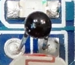
Thermistor – The thermistor is a resistor that changes resistance based on temperature.
A decrease in temperature will cause the voltage to increase on channel 1.
The thermistor is useful for detecting changes in temperature. Since the specification of the thermistor is not known so it is difficult to use it to measure the actual temperature. It is better suited for measuring relative changes in temperature and in some cases the readings can be correlated to a temperature by empirical testing.
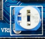
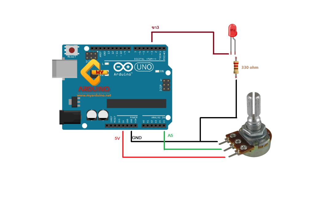
Potentiometer – The 10K potentiometer is connected between Vcc and Gnd with the wiper connected to channel 3.
Rotating the potentiometer will cause the voltage to vary between 0V and Vcc. Rotating the potentiometer CW decreases the voltage on channel 3.
The potentiometer can be used as a general purpose analog control input. For instance, the potentiometer can be read and the DAC output driving the LED can be set to match the read value.
I2C Interface
I2C Address
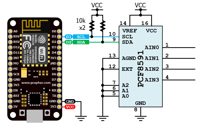
The module has a fixed I2C address of 0x48. The chip itself has 3 address pins but they are all tied to ground on the module, so it is not adjustable.
I2C Pull-Up Resistors
The module includes two 10K pull-up resistors on the I2C SCL and SDA lines.
Module Connections
The connections to the module are fairly simple.
- Supply 3.3 or 5V power to match the MCU power and ground.
- Connect I2C SCL and SDA lines to same on the MCU.
1 x 4 Header
- SCL = I2C SCL connects to MCU SCL
- SDA = I2C SDA connects to MCU SDA
- GND = Ground connects to MCU ground
- VCC = Power (2.5 to 6V). Typically connects to same power as MCU.
1 x 5 Header
- AOUT = DAC analog output
- AIN0 = ADC channel 0 input
- AIN1 = ADC channel 1 input
- AIN2 = ADC channel 2 input
- AIN3 = ADC channel 3 input
OUR EVALUATION RESULTS:
These modules have fair build quality and are easy to use for demonstrating analog input and analog output concepts. It can also be handy in small applications where you need some or all of the functionality that it provides.
The main limitation is that the ADC and DAC are 8-bit which is relatively low and may be a limitation for some applications. Having a fixed I2C address is not usually an issue for the type of applications this module is suitable for, but if it is desired to use two modules, it would require a 2nd I2C bus.
The test program here uses the library by Rob Tillaart which can be downloaded via the Library Manager in the Arduino IDE.
The connections are simple, just connect the module I2C SDA and SCL lines to the corresponding MCU SDA and SCL lines. Also apply 5V or 3.3V power to match your MCU and ground. If you are powering the module from 5V, you can connect 3.3V to the channel 2 (AIN2) header pin to have something to read on that channel.
The program below is designed to test the basic features of the module. It first exercises the DAC output by ramping the brightness of the on-board green LED up and then back down. The four analog inputs are then read. If you have the jumpers installed, it will read the LDR, thermistor and potentiometer. If the jumpers are removed it will read the voltage on the header pins instead.
When the appropriate section of the program is executing, you can shield the LDR or shine a light on it to see the change. The thermistor can be warmed with your fingers and the potentiometer can be adjusted to see the effect. On the unassigned AIN2 pin, the program converts the reading to a voltage. If you connect it to 3.3V, you should see a reading of between about 3.15V and 3.45V
In our test program, we use the MAP function to reverse the functionality of the LDR and thermistor so that they both increase in value as the light or temperature increases as you would normally expect. It is not really necessary, but it makes these sensor inputs react more intuitively.
PCF8591 A/D and D/A Converter Module Test Program
/*  PCF8591 Module Test Program
 *   CH0 = Photoresistor Input
 *   CH1 = Thermistor temperature input
 *   CH2 = Unassigned analog input
 *   CH3 = Potentiometer Input
 *
 *   Connect I2C SCL/SDA and power/ground
 *   Uses Rob Tillaart library.  URL: https://github.com/RobTillaart/PCF8591
*/

#include "PCF8591.h"
#include "Wire.h"
PCF8591 dev(0x48);
//===============================================================================
//  Initialization
//===============================================================================
void setup()
{
  Serial.begin(9600);
  Wire.begin();
  dev.begin();
}
//===============================================================================
//  Main
//===============================================================================
void loop()
{
//  Test D/A output
  Serial.println("D/A Output Test - Ramp LED up/down");
 // dev.enableDAC();                // Enable DAC output
  for (int i = 0; i < 256; i++)   // Ramp voltage / LED brightness UP
  {
    Serial.println(i);
    dev.analogWrite(i);
    delay(15);                    // just to slow the effect
  }

  for (int i = 255; i >= 0; i--)  // Ramp voltage / LED brightness DOWN
  {
    Serial.println(i);
    dev.analogWrite(i);
    delay(15);
  }
//  dev.disableDAC(); // Disable DAC output

// Test Ch0 LDR
  Serial.println("Ch 0 LDR Light Test");
  for (int i= 0; i<30; i++)     // Take 30 readings
  {
    byte ch0 = dev.analogRead(0); // Read LDR sensor input
    ch0 = map(ch0, 0,255, 255, 0); // Map reading so brighter = higher value
    Serial.println(ch0);  // Shield sensor to see change
    delay(350);
  }

// Test Ch1 Thermistor
  Serial.println("Ch 1 Thermistor Temperature Test");
  for (int i= 0; i<30; i++)
  {
    byte ch1 = dev.analogRead(1); // Read Thermistor sensor input
    ch1 = map(ch1, 0,255, 255, 0); //Map reading so warmer = higher value
    Serial.println(ch1);  // Warm sensor to see change
    delay(350);
  }

// Test Ch2 Analog Input
  Serial.println("Ch 2 Analog Input Test");  // Read analog 2 input
  for (int i= 0; i<30; i++)              // Connect to 3.3V to see difference
  {
    byte ch2 = dev.analogRead(2);
    float voltage = ch2 * (5.0 / 256.0);  // Convert reading to voltage
    Serial.println(voltage);
    delay(350);
  }

// Test Ch3 Potentiometer
  Serial.println("Ch 3 Potentiomter Test"); // Read potentiometer input
  for (int i= 0; i<30; i++)
  {
    Serial.println(dev.analogRead(3));      // Read and print value from pot
    delay(350);
  }
}
Link: https://www.esp8266learning.com/wemos-pcf8591-example
https://protosupplies.com/product/pcf8591-a-d-and-d-a-converter-module/